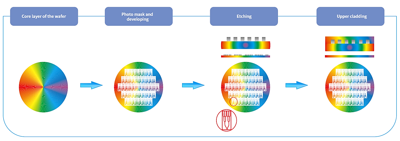
Based on Planar Lightwave Circuit technologies, PLC splitter wafers are produced on the quartz substrate through a series of processes including CVD deposition, photo-masking, etching, etc. PLC splitter wafers can be designed for 1x2, 1x4, 1x8, 1x16, 1x32, 1x64 and 2xN. Splitter chips with high yield, quality and reliability, are made of PLC wafers through dicing and polishing.
The processes for the PLC splitter wafers include CVD deposition on the substrate, photo-masking, developing, and etching to form the pattern of waveguide circuit, and finally an upper cladding film is deposited to protect the waveguide.
Optical communication networks, Telecom equipment, Three-Network-Integration systems, including Signal/power distribution, Fiber-To-The-Home (FTTH), Passive Optical Network (PON).


 Fiber Optic Flex Circuit (FOFC)
Advanced Simulation & Optimization, High Positioning Accuracy, Flexible Customization, Rigorous Reliability Testing
 MDC Solution
US Conec's MDC connector is a Very Small Form Factor (VSFF) duplex optical connector, expertly designed for terminating single-mode and multimode fiber cables with diameters up to 2.0mm.
 MMC Solution
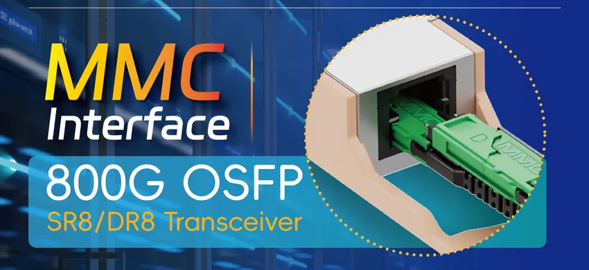
US Conec's Very Small Form Factor (VSFF) multi-fiber optical connector that redefines high-density connectivity with its cutting-edge TMT ferrule technology and intuitive Direct-Conec™ push-pull boot design.
 EN
EN
 jp
jp  fr
fr  es
es  it
it  ru
ru  pt
pt  ar
ar  el
el  nl
nl 
