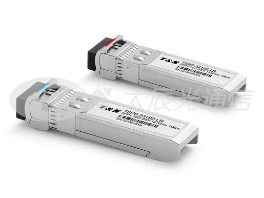
The TSPB-23192-LR & TSPB-32192-LR Series single mode transceiver is small form-factor pluggable module for duplex optical data communications such as 10GBASE-LR/LW defined by IEEE 802.3ae. It is with the SFP+ 20-pin connector to allow hot plug capability.
The TSPB-23192-LR module is designed for single-mode fiber and operates at a nominal wavelength of 1270nm; TSPB-32192-LR module is designed for single-mode fiber and operates at a nominal wavelength of 1330nm. The transmitter section uses a multiple quantum well DFB, which is class 1 laser compliant according to International Safety Standard IEC-60825.
The receiver section uses an integrated InGaAs detector preamplifier (IDP) mounted in an optical header and a limiting post-amplifier IC.
Simplex LC Connector Bi-Directional SFP+ Optical Transceiver
Compliant with SFF-8431, SFF-8432 and IEE802.3ae
Up to 10km on 9/125um SMF
Two types:
A:1270nm DFB Laser transmitter,1330nm receiver
B:1330nm DFB Laser transmitter,1270nm receiver
Digital Diagnostic SFF-8472 Compliant
Operating case temperature 0 ~ 70 °C
RoHS6 compliant (lead-free)
10GBASE-LR at 10.3125Gbps
Other Optical Links
These values represent the damage threshold of the module. Stress in excess of any of the individual Absolute Maximum Ratings can cause immediate catastrophic damage to the module even if all other parameters are within Recommended Operating Conditions.
Parameters | Symbol | Min. | Max. | Unit |
Supply Voltage | VCC | -0.5 | +3.6 | V |
Storage Temperature | Tc | -40 | +85 | °C |
Operating Case Temperature | Tc | 0 | +70 | °C |
Relative Humidity | RH | 0 | 85 | % |
Parameters | Symbol | Min. | Typical | Max. | Unit |
Supply Voltage | VCC | 3.0 | 3.3 | 3.6 | V |
Supply current | Icc | 200 | 300 | mA | |
Operating Case Temperature | TC | 0 | 25 | 70 | °C |
Module Power Dissipation | Pm | - | 0.7 | 1.1 | W |
Notes:
Supply current is shared between VCCTX and VCCRX.
In-rush is defined as current level above steady state current requirements.
Parameter | Symbol | Min. | Typical | Max | Unit | Ref. |
Supply Voltage | VCC | 3.00 | 3.60 | V | 1 | |
Supply Voltage | Icc | 200 | 300 | mA | 1 | |
Transmitter | ||||||
Input differential impedance | Rin | 100 | Ω | 2 | ||
Single ended data input swing | Vin,pp | 150 | 1200 | mVpp | ||
Transmit Disable Voltage | VD | 2 | VCC | V | ||
Transmit Enable Voltage | VEN | Vee | Vee+0.8 | V | 3 | |
Receiver | ||||||
Output differential impedance | Rout | 100 | Ω | 2 | ||
Single ended data output swing | Vout,pp | 300 | 700 | mV | 4 | |
LOS Fault | VLOS fault | 2 | VCCHOST | V | 5 | |
LOS Normal | VLOS norm | Vee | Vee+0.8 | V | 5 | |
Notes:
Module power consumption never exceeds 1W.
AC coupled.
Or open circuit.
Into 100 ohm differential termination.
LOS is LVTTL. Logic 0 indicates normal operation; logic 1 indicates no signal detected.
Parameter | Symbol | Min. | Typical | Max | Unit | Ref. |
Transmitter | ||||||
Optical Wavelength | λC | 1260 | 1270 | 1280 | nm | |
Side Mode Suppress Ratio | SMSR | 30 | dB | |||
Spectral Width(-20dB) | Δλ | 1 | nm | |||
Average Output Power | Pop | -8.2 | 0.5 | dBm | 1,2 | |
Extinction Ratio | ER | 3.5 | dB | |||
Eye Mask | Compliant with IEEE 802.3 | |||||
Receiver | ||||||
Average Receiver Power | RSENS | -14.1 | dBm | 2,3 | ||
Receiver Overload | PMAX | +0.5 | dBm | |||
Centre Wavelength | λC | 1320 | 1340 | nm | ||
LOS De-Assert | LOSD | -15 | dBm | |||
LOS Assert | LOSA | -30 | dBm | |||
LOS Hysteresis | 0.5 | dB | ||||
Parameter | Symbol | Min. | Typical | Max | Unit | Ref. |
Transmitter | ||||||
Optical Wavelength | λC | 1320 | 1330 | 1340 | nm | |
Side Mode Suppress Ratio | SMSR | 30 | dB | |||
Spectral Width(-20dB) | Δλ | 1 | nm | |||
Average Output Power | Pop | -8.2 | 0.5 | dBm | 1,2 | |
Extinction Ratio | ER | 3.5 | dB | |||
Eye Mask | Compliant with IEEE 802.3 | |||||
Receiver | ||||||
Average Receiver Power | RSENS | -14.1 | dBm | 2,3 | ||
Receiver Overload | PMAX | +0.5 | dBm | |||
Centre Wavelength | λC | 1260 | 1270 | nm | ||
LOS De-Assert | LOSD | -15 | dBm | |||
LOS Assert | LOSA | -30 | dBm | |||
LOS Hysteresis | 0.5 | dB | ||||
Notes:
Output is coupled into a 9/125um SMF.
Average Receiver Power (Min) is informative and not the principal indicator of signal strength. A received power below this value cannot be compliant.
Measured with a PRBS231-1 test pattern @10.3125Gbps, BER≦10-12

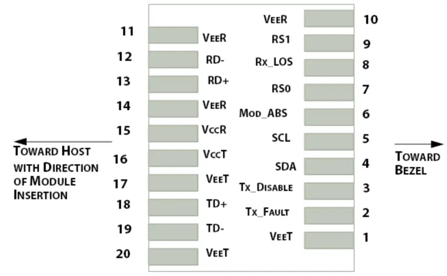
Pin | Symbol | Name/Description |
1 | VEET [1] | Transmitter Ground |
2 | Tx_FAULT [2] | Transmitter Fault |
3 | Tx_DIS [3] | Transmitter Disable. Laser output disabled on high or open |
4 | SDA [2] | 2-wire Serial Interface Data Line |
5 | SCL [2] | 2-wire Serial Interface Clock Line |
6 | MOD_ABS [4] | Module Absent. Grounded within the module |
7 | RS0 [5] | RS0 for Rate Select: Open or Low = Module supports ≤4.25Gbps High = Module supports 9.95 Gb/s to 10.3125 Gb/s |
8 | RX_LOS [2] | Loss of Signal indication. Logic 0 indicates normal operation |
9 | RS1 [5] | No connection required |
10 | VEER [1] | Receiver Ground |
11 | VEER [1] | Receiver Ground |
12 | RD- | Receiver Inverted DATA out. AC Coupled |
13 | RD+ | Receiver DATA out. AC Coupled |
14 | VEER [1] | Receiver Ground |
15 | VCCR | Receiver Power Supply |
16 | VCCT | Transmitter Power Supply |
17 | VEET [1] | Transmitter Ground |
18 | TD+ | Transmitter DATA in. AC Coupled |
19 | TD- | Transmitter Inverted DATA in. AC Coupled |
20 | VEET [1] | Transmitter Ground |
Notes:
Module circuit ground is isolated from module chassis ground within the module.
should be pulled up with 4.7k – 10k ohms on host board to a voltage between 3.15Vand 3.6V.
Tx_Disable is an input contact with a 4.7 kΩ to 10 kΩ pullups to VccT inside the module.
Mod_ABS is connected to VeeT or VeeR in the SFP+ module. The host may pull this contact up to Vcc_Host with a resistor in the range 4.7 kΩ to10 kΩ.Mod_ABS is asserted “High” when the SFP+ module is physically absent from a host slot.
RS0 and RS1 are module inputs and are pulled low to VeeT with > 30 kΩ resistors in the module.
T&S SFP+ transceiver is designed to be Class I Laser safety compliant and is certified per the following standards:
Feature | Agency | Standard | Certificate / Comments |
Laser Safety | FDA | CDRH 21 CFR 1040 and Laser Notice No. 50 | 1120292-000 |
Product Safety | UL | UL and CUL EN60950-2:2007 | E347511 |
Environmental protection | SGS | RoHS Directive 2002/95/EC | GZ1001008918/CHEM |
EMC | WALTEK | EN 55022:2006+A1:2007 EN 55024:1998+A1+A2:2003 | WT10093759-D-E-E |
"Specifications for Enhanced Small Form Factor Pluggable Module SFP+", SFF-8431, Rev 4.1, July 6, 2009
"Improved Pluggable Formfactor", SFF-8432, Rev 4.2, Apr 18, 2007
IEEE802.3ae – 2002
"Diagnostic Monitoring Interface for Optical Transceivers" SFF-8472, Rev 10.3, Dec 1,2007
Performance figures, data and any illustrative material provided in this data sheet are typical and must be specifically confirmed in writing by T&S before they become applicable to any particular order or contract. In accordance with the T&S policy of continuous improvement specifications may change without notice.
The publication of information in this data sheet does not imply freedom from patent or other protective rights of T&S or others. Further details are available from any T&S sales representative.
 Industrial 5G: Transforming Manufacturing and Automation in the Era of Industry 4.0
17 Jan 2024
In the rapidly advancing landscape of technology, the rise of Industry 4.0 has introduced unprecedented connectivity and automation. At the forefront of this transformative wave is Industrial 5G—a so...
 Call us on:
  Email Us:
  8 Jinxiu Middle Road,