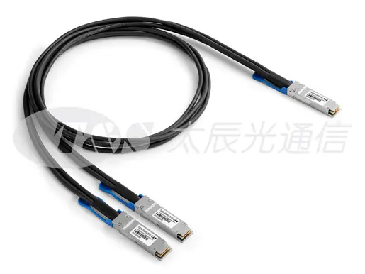
QSFP56 passive copper cable assembly feature eight differential copper pairs, providing four data transmission channels at speeds up to 56Gbps(PAM4) per channel, and meets 200G Ethernet and InfiniBand requirements. Available in a broad rang of wire gages-from 26AWG through 30AWG-this 200G copper cable assembly features low insertion loss and low cross talk.
QSFP56 uses PAM4 signals for transmission, which doubles the rate. However, there are more stringent requirements for cable insertion loss. For detailed requirements, please see High Speed Characteristics.
Designed for applications in the data center, networking and telecommunications markets that require a high speed, reliable cable assembly, this next generation product shares the same mating interface with QSFP+ form factor, making it backward compatible with existing QSFP ports.
Compatible with IEEE 802.3bj and IEEE 802.3cd
Supports aggregate data rates of 200Gbps(PAM4)
Optimized construction to minimize insertion loss and cross talk
Pull-to-release slide latch design
28AWG through 30AWG cable
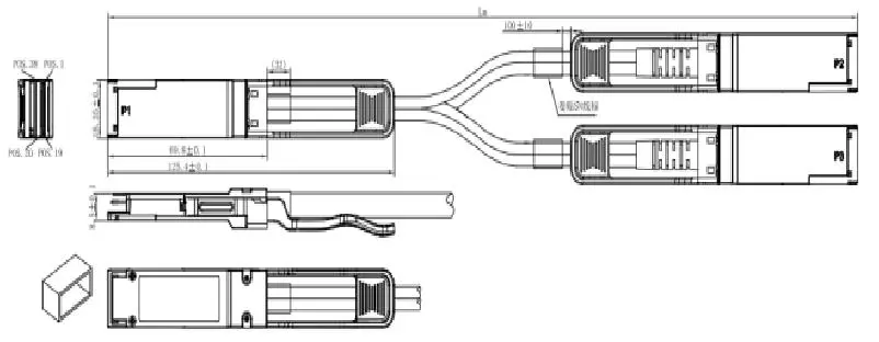
Straight and break out assembly configurations available
Customized cable braid termination limits EMI radiation
Customizable EEPROM mapping for cable signature
RoHS Compatible
Switches, servers and routers
Data Center networks
Storage area networks
High performance computing
Telecommunication and wireless infrastructure
Medical diagnostics and networking
Test and measurement equipment
200G Ethernet (IEEE 802.3cd)
InfiniBand
Parameter | Symbol | Min | Max | Unit |
Operating Case Temperature | Topc | 0 | 70 | degC |
Storage Temperature | Tst | -40 | 85 | degC |
Relative Humidity (non-condensation) | RS | 35 | 60 | % |
Supply Voltage | VCC3 | 3.135 | 3.465 | V |
Voltage on LVTTL Input | Vilvttl | -0.3 | VCC3 +0.2 | V |
Power Supply Current | ICC3 | - | 15 | mA |
Total Power Consumption | Pd | - | 0.05 | W |
Notes:
Stress or conditions exceed the above range may cause permanent damage to the device.
This is a stress rating only and functional operation of the device at these or any other conditions above those listed in the operational sections of this specification is not applied. Exposure to absolute maximum rating conditions for extended periods may affect device reliability.
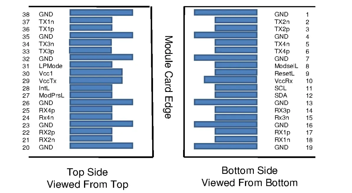
Pin | Logic | Symbol | Description |
1 | - | GND | Ground |
2 | CML-I | Tx2n | Transmitter Inverted Data Input |
3 | CML-I | Tx2p | Transmitter Non-Inverted Data Input |
4 | - | GND | Ground |
5 | CML-I | Tx4n | Transmitter Inverted Data Input |
6 | CML-I | Tx4p | Transmitter Non-Inverted Data Input |
7 | - | GND | Ground |
8 | LVTTL-I | ModSelL | Module Select |
9 | LVTTL-I | ResetL | Module Reset |
10 | - | Vcc Rx | +3.3V Power Supply Receiver |
11 | LVCMOS- | SCL | 2-wire serial interface clock |
I/O | |||
12 | LVCMOS- | SDA | 2-wire serial interface data |
I/O | |||
13 | - | GND | Ground |
14 | CML-O | Rx3p | Receiver Non-Inverted Data Output |
15 | CML-O | Rx3n | Receiver Inverted Data Output |
16 | - | GND | Ground |
17 | CML-O | Rx1p | Receiver Non-Inverted Data Output |
18 | CML-O | Rx1n | Receiver Inverted Data Output |
19 | - | GND | Ground |
20 | - | GND | Ground |
21 | CML-O | Rx2n | Receiver Inverted Data Output |
22 | CML-O | Rx2p | Receiver Non-Inverted Data Output |
23 | - | GND | Ground |
24 | CML-O | Rx4n | Receiver Inverted Data Output |
25 | CML-O | Rx4p | Receiver Non-Inverted Data Output |
26 | - | GND | Ground |
27 | LVTTL-O | ModPrsL | Module Present |
28 | LVTTL-O | IntL | Interrupt |
29 | - | Vcc Tx | +3.3V Power supply transmitter |
30 | - | Vcc1 | +3.3V Power supply |
31 | LVTTL-I | LPMode | Low Power Mode |
32 | - | GND | Ground |
33 | CML-I | Tx3p | Transmitter Non-Inverted Data Input |
34 | CML-I | Tx3n | Transmitter Inverted Data Input |
35 | - | GND | Ground |
36 | CML-I | Tx1p | Transmitter Non-Inverted Data Input |
37 | CML-I | Tx1n | Transmitter Inverted Data Input |
38 | - | GND | Ground |
Parameter | Symbol | Min | Typical | Max | Unit | Note |
Differential Impedance | TDR | 90 | 100 | 110 | Ώ | - |
Insertion loss | SDD21 | -16.06 | - | - | dB | At 13.28 GHz |
Differential Return Loss | SDD11 SDD22 | - | - | See 1 | dB | At 0.05 to 4.1 GHz |
- | - | See 2 | dB | At 4.1 to 19 GHz | ||
Common-mode to common-mode output return loss | SCC11 SCC22 | - | - | -2 | dB | At 0.2 to 19 GHz |
Differential to common-mode return loss | SCD11 SCD22 | - | - | See 3 | dB | At 0.01 to 12.89 GHz |
- | - | See 4 | At 12.89 to 19 GHz | |||
Differential to common Mode Conversion Loss | SCD21-IL | - | - | -10 | dB | At 0.01 to 12.89 GHz |
- | - | See 5 | At 12.89 to 15.7 GHz | |||
- | - | -6.3 | At 15.7 to 19 GHz |
Notes:
1. Reflection Coefficient given by equation SDD11(dB) < -16.5 + 2 × SQRT(f ), with f in GHz
2. Reflection Coefficient given by equation SDD11(dB) < -10.66 + 14 ×logo10/5.5, with f in GHz
3. Reflection Coefficient given by equation SCD11(dB) < -22 + (20/25.78)*f, with f in GHz
4. Reflection Coefficient given by equation SCD11(dB) < -15 + (6/25.78)*f, with f in GHz
Reflection Coefficient given by equation SCD21(dB) < -27 + (29/22)*f, with f in GHz

The connector is compatible with the SFF-8436 specification.

Length (m) | Cable AWG |
1 | 30 |
2 | 26/30 |
3 | 26 |
Feature | Test Method | Performance |
Electrostatic Discharge (ESD) to the Electrical Pins | MIL-STD-883C Method 3015.7 | Class 1(>2000 Volts) |
Electromagnetic Interference(EMI) | FCC Class B | Compliant with Standards |
CENELEC EN55022 Class B | ||
CISPR22 ITE Class B | ||
RF Immunity(RFI) | IEC61000-4-3 | Typically Show no Measurable Effect from a 10V/m Field Swept from 80 to 1000MHz |
RoHS Compliance | RoHS Directive 2011/65/EU and it's Amendment Directives 6/6 | RoHS 6/6 compliant |
 PLC Optical Splitter vs FBT Optical Splitter: What's the Difference?
08 Jul 2022
An optical splitter is a passive optical device that can split an input optical signal into multiple output optical signals, and is widely used in passive optical fiber networks. According to the diff...
 Call us on:
  Email Us:
  8 Jinxiu Middle Road,